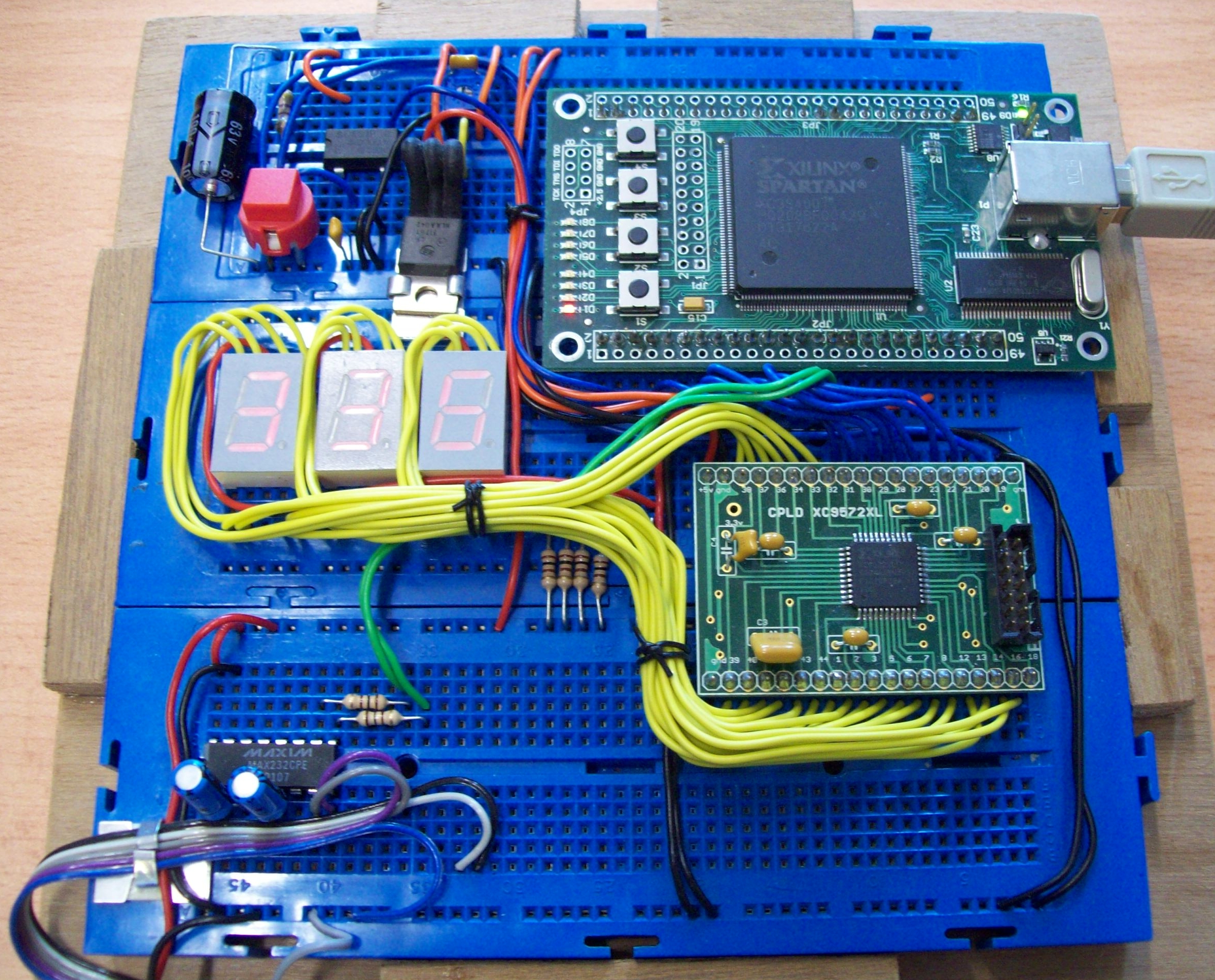
Figure 1 : PicoBlaze stopwatch
Always thought that this looked like a Hollywood bomb, lots of flashing lights, LED display counting down, a man posed to cut the red wire etc. In reality its even more dramatic a teaching demo to illustrate the differences between polling and interrupts. Its also a good test to see if you really do understand how a basic computer works. Originally called the (K)constant Coded Programmable State Machine (KCPSM), Xilinx's PicoBlaze CPU is an eight bit, soft core processor, that i use as a test platform to introduce assembly language programming. The CPU comes in a number of different flavours, but i tend to use PicoBlaze version 3, as it has a nice clean instruction set / architecture, ideal when your programming at this level for the first time. More details on its architecture can be found here: (Link). The PicoBlaze can not be purchased as an IC, it is defined using a Hardware Description Language (HDL). There are a number of different types of HDLs, but for low level (RTL) hardware design i use VHDL (Very High Speed IC HDL). More information on this language can be found here: (Link) (Local), (Link). The PicoBlaze's HDL representation can be simulated on a computer to see if the hardware model is 'correct', it can then be converted into a configuration file and 'downloaded' into a programmable logic device, in this can an Opal Kelly Spartan 3 FPGA board (Link). For more background info on FPGAs refer to: (Link)(Local). I could of implemented the complete system using this one device, but i decided to separate out the LED display storage into a CPLD (Link), another type of programmable hardware device, to illustrate how data is communicated across a simple bus.
System
Simple Output Port
Time delay
Simple Input Port
Binary to Decimal Conversion
Seven Segment Display
Complex Output Port
Final System
This system has three seven-segment LED displays, allowing it to display a value from 000 to 999 seconds. Controlling this counter are three switches. The RESET switch resets the PicoBlaze, resetting the count to zero. To stop the count at its present value there are two STOP buttons. One button is interfaced to the processor using an input port i.e. polled, the other is connected to the processor using the interrupt line.
LIBRARY IEEE;
USE IEEE.STD_LOGIC_1164.ALL;
ENTITY system IS
PORT (
clk_i : IN STD_LOGIC;
rst_i : IN STD_LOGIC;
po_A_dat_o : OUT STD_LOGIC_VECTOR(3 DOWNTO 0);
po_A_adr_o : OUT STD_LOGIC_VECTOR(2 DOWNTO 0);
po_A_en_o : OUT STD_LOGIC;
pi_B_dat_i : IN STD_LOGIC_VECTOR(3 DOWNTO 0);
po_C_dat_o : OUT STD_LOGIC_VECTOR(7 DOWNTO 0) );
END system;
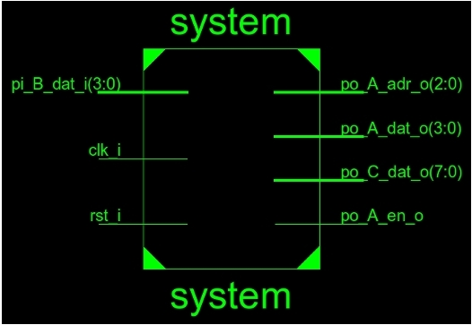
Figure 2 : Top level system interface, circuit symbol (top), VHDL (bottom)
The top level interface of the PicoBlaze system within the FPGA i.e. the physical wires connected to the bread board (outside world), are the Input / Output (IO) ports A,B and C, are shown in figure 2. There are two types of ports (connections) used STD_LOGIC: a single wire i.e. a signal and STD_LOGIC_VECTOR: a group of wires i.e. a bus. These can be either inputs that the CPU can read or outputs that the CPU can write to (control).
Like most CPUs the PicoBlaze has no idea about IO ports, all it can do is read or write to different data memory locations. The PicoBlaze has a whooping 256 bytes of data memory, not Gig, Meg or K, just 256 bytes. From some points of view this can be considered a limitation, however, this processor was never designed to be a number cruncher i.e. process images, it is intended to be used in small embedded applications where this amount of data memory is perfectly fine, also it does have an additional 64 bytes of scratchpad memory :). To 'connect' these memory locations to the outside world you need an IO peripheral, these can be simple e.g. buffers or flip-flops, or more complex, having their own thread of control e.g. serial port communications. In this system Port C is a simple 8bit output port, the 8bit value the CPU writes to its memory location drives an 8bit value (wires) in the real world. When the system was designed this port was assigned the memory address 80 decimal, which is the same as 0x50 hexadecimal, or 01010000b binary. A memory location is identified by its address (number), the PicoBlaze can address memory locations 0 to 255 (in hex this would be 0x00 to 0xFF). Remember you can change the base used to represent an address e.g. decimal(10), octal(8) or hexadecimal(16), but the memory location is the same, it will always be the same binary(2) pattern. To illustrate the steps involved in writing to a IO peripheral consider the stripped down system shown in figure 3, i.e. only has port C.
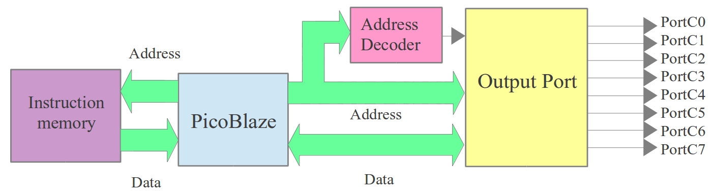
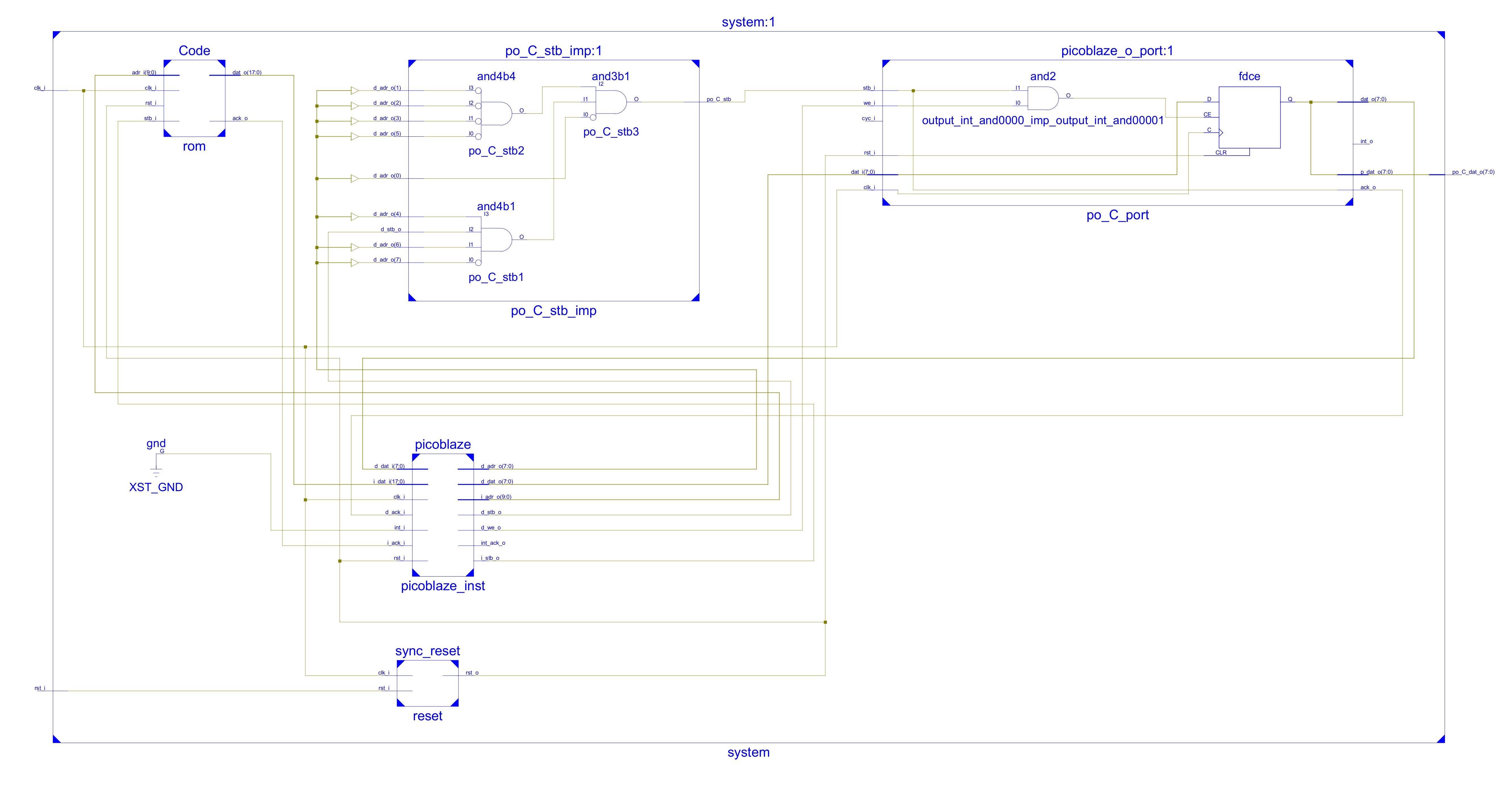
Figure 3 : Simplified system, block diagram (top), RTL schematic (bottom)
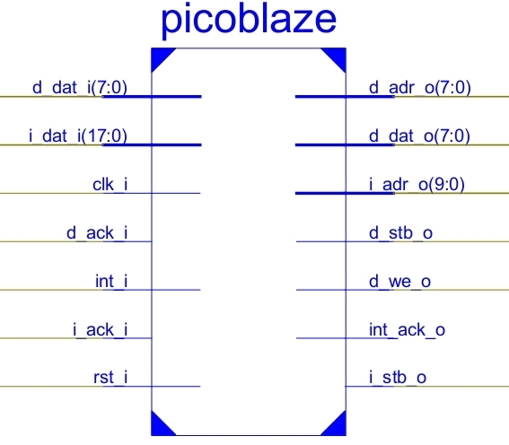
Figure 4 : PicoBlaze CPU
These circuit diagrams (schematics) are automatically generated from the VHDL and give a good overview of what is connected to what. At the heart of the system is the PicoBlaze CPU shown in figure 4. This is a Harvard processor i.e. has physically separate memories for instructions and data. The PicoBlaze's interface is roughly based on the WishBone system bus, for more information on how this operates refer to: (Link)(Local), (Link) (Local).
On the PicoBlaze the only instructions that can read or write to a data memory location are IN and OUT, consider the simple program below:
; *==========================================================
; * CONSTANT
; *==========================================================

	PortC  EQU 0x50;

; *==========================================================
; * MAIN
; *==========================================================

start:
        LOAD S0, 1        ;count
loop:
        OUT S0, PortC     ;write count to port
        IN S1, PortC      ;read port, store data in register
        ADD S1, 1         ;add 1 to register
        LOAD S0, S1       ;transfer incremented value to count

        JUMP loop
A simulation of this program running on this hardware is shown in figure 5. This program initialises a register (S0) with the value 1 (COUNT), this is then written to output port C. In the program PortC is a symbolic label for the address constant 0x50, defined by the assembler directive EQU. This OUT instruction triggers a write operation on the PicoBlaze's data bus as shown in 6. The CPU places the address of Port C (0x50) on the address bus (d_adr_o) and the data it wishes to store (0x01) on the data bus (d_dat_o). It then sets the data strobe line (d_stb_o) and write enable line (d_we_o) high to signal that a memory write transaction has started. The output port's hardware detects this and updates its output (po_c_dat_o) to this new value (0x01) and signals it has completed this request by setting the acknowledge line high (d_ack_i). Next, the program reads the data stored in the output port using an IN instruction. This triggers a read operation on the PicoBlaze's data bus as shown in 7. Again the CPU places the address of Port C (0x50) on the address bus (d_adr_o). It then sets the data strobe line (d_stb_o) high and write enable line (d_we_o) low to signal that a memory read transaction has started. The output port's hardware detects this and outputs its data (0x01), signalling it has completed this request by setting the acknowledge line high (d_ack_i). The program then adds 1 to this value, updates the variable COUNT and then repeats. This program could be optimised to remove the IN and LOAD instructions, but they do help illustrate a common misunderstanding made when programming the PicoBlaze: IN instructions read external data (memory), LOAD instructions read internal data (constants or registers) i.e. you can not use a LOAD instruction to read a memory location.
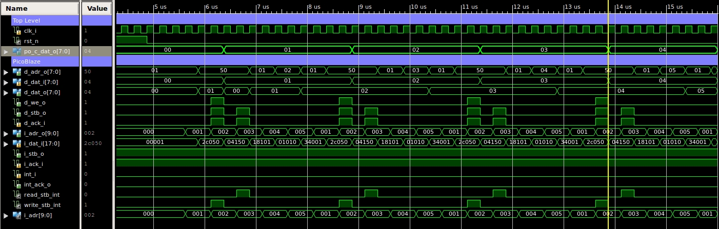
Figure 5: Test code 1 simulation
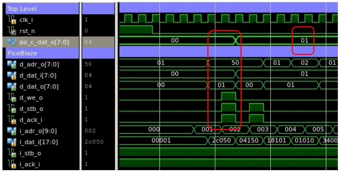
Figure 6: Data memory write
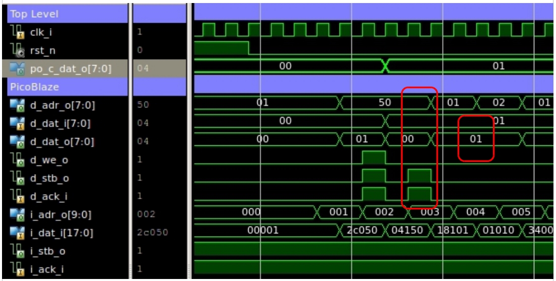
Figure 7: Data memory read
In addition to showing data memory transactions, figure 5 also shows instruction fetches i.e. the instruction memory address bus (i_adr_o) and data bus (i_dat_o). Looking at these buses you can disassemble the machine code i.e. match the machine code numbers to the assembly language text:
Start:
	LOAD S0, 1	 ADDR:0  DATA:00001
Loop:
	OUT S0, 0x50	 ADDR:1  DATA:2C050
	IN S1, 0x50	 ADDR:2  DATA:04150
	ADD S1, 0x01	 ADDR:3  DATA:18101
	LOAD S0, S1	 ADDR:4  DATA:01010
	JUMP 0x01	 ADDR:5  DATA:34001
A more detailed explanation of the Wishbone bus read / write operations can be found in the specification links above.
Hopefully the previous description has explained what happens on the PicoBlaze's buses when the IN and OUT instructions are executed, but how does the output port know it needs to respond to these read or write transactions? How does it store its data? This is decided by the address decoding hardware, as shown in figure 8. Each peripheral is assigned an unique address, its address decoding hardware only outputs a logic 1 when its address is on the processor's address bus (d_adr_o). The output port used in the previous examples is assigned the address 0x50 or 01010000 in binary, therefore, the address decoder will only produce a logic 1 when:
Note, the circles on some of the AND gate inputs infer an inverter. Within the output port, shown in figure 9, the address decoder's output is ANDed with the write enable line (d_we_o), controlling the Clock Enable (CE) line on the 8bit flip-flop (Link). Therefore, when the processor writes to this memory location the data on the data bus (d_dat_o) will be stored in the output ports eight internal flip-flops. The Q outputs of which drive Port C shown in figure 2.
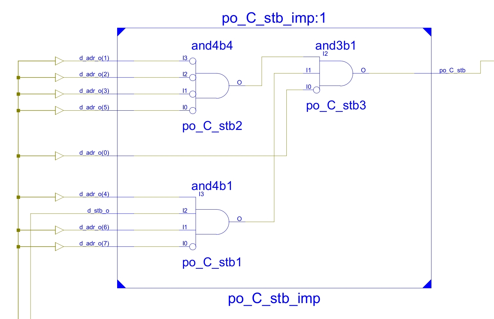
Figure 8 : Address decoder
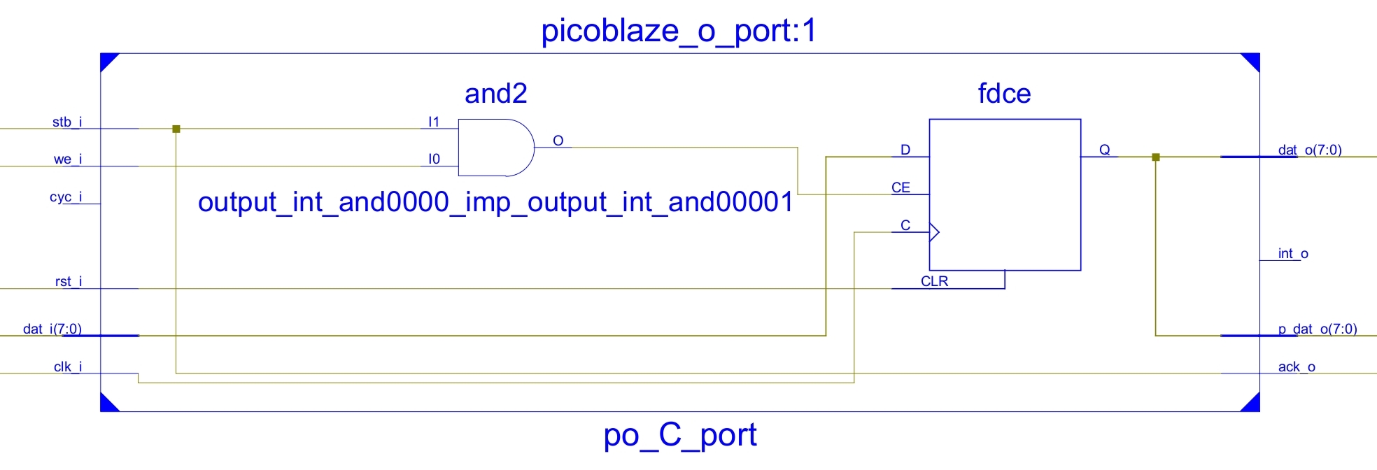
Figure 9 : Output port
In the stopwatch system shown in figure 1, port C is used to control the eight LEDs on the Opal Kelly Spartan 3 FPGA board. Each LED is configured as shown in figure 10. A logic 1 turns off an LED as there will be no potential difference across it (the LED is not forward biased). A logic 0 will turn on an LED as there is more than the 2V needed across the LED for current to flow.
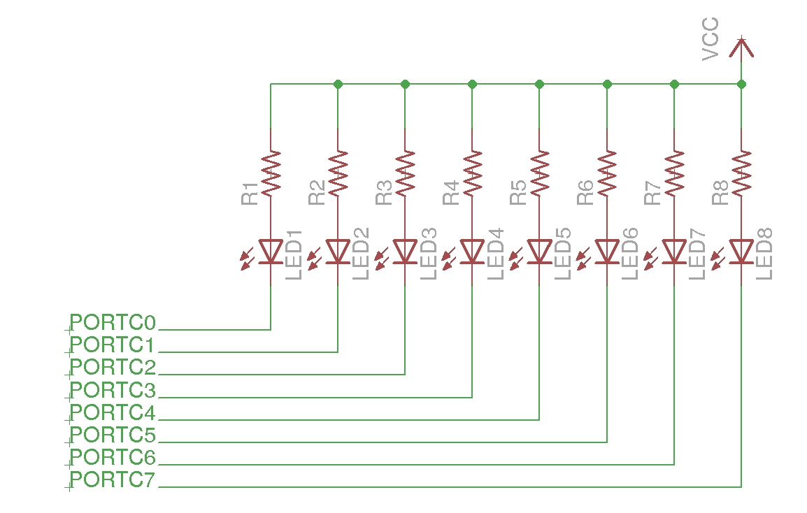
Figure 10 : Output LEDs
To implement a 1 second delay the delay subroutine shown below is used. In a real stopwatch this delay would be implemented using a Periodic Interrupt Timer (PIT) i.e. a hardware counter, dividing the system clock down to a lower frequency, implementing a real-time clock. However, the aim of this project was to show the difference between a polling and interrupt based inputs, therefore, by using this software based solution the polled STOP button will only be tested approximately once per second. The state of the software delay loop is displayed on the eight LEDs connected to port C. Initially all LEDs are off. As the delay progresses LEDs are incrementally turn on, to form a bar-graph type display (thermometer scale encoded). The state of the LEDs is stored in register SB, initially this is set to all 1's i.e. 0xFF, turning off all the LEDs. The software delay is implemented using three nested loops controlled by registers SC, SD and SE. The inner loop decrements SE from 256 to 0, it then decrements SD by 1, and repeats. This continues until SC is zero. The value in SB is then shifted left, inserting a zero and stored in port C i.e. turns on an LED. The program checks to see if all LEDs have been turn on, if it has the delay subroutine exits, otherwise it repeats. The PicoBlaze's system clock is running at 4Mhz and each instruction takes 2 cycles, to produce a delay of approximately 1 second you would need to use the following values:
DELAY = ((((((0x100*4)+4)*0xF3)+6)*2)+12)*8) / 4000000 = 3997056 / 4000000 = 0.99926 seconds
; *==========================================================
; * CONSTANT
; *==========================================================

	LED_PORT  EQU 0x50;

; *==========================================================
; * DELAY
; *==========================================================

delay:	LOAD SE, 0x00        ;set initial count value
	LOAD SD, 0xD7
	LOAD SC, 0x02
	LOAD SB, 0xFF	     ;set all LEDs to off

delay_loop:
	SUB SE, 1            ;inner loop
	JUMP NZ, delay_loop
	SUB SD, 1            ;middle loop
	JUMP NZ, delay_loop

	LOAD SD, 0xD7
	SUB SC, 1            ;outer loop
	JUMP NZ, delay_loop

	LOAD SC, 0x02
	AND SB, 0xFF         ;have all LEDs been turned on?
        RET Z                ;yes, exit

	SL0 SB               ;no, turn on the next LED
	OUT SB, LED_PORT     ;update Port
	JUMP delay_loop      ;repeat
However, if you were to uses these values i.e. SE=0x00, SD=0xF3 and SC=0x02 the stopwatch will be slow as you also need to take into account the software delays associated with updating the display etc. Therefore, with a bit of trial and error, the values SE=0x00, SD=0xD7 and SC=0x02 were selected (timed over a minute). Note, this will never be perfect as the path through the program (delays) are data dependent. A video of this time delay subroutine and LED control in action is here: (Video)
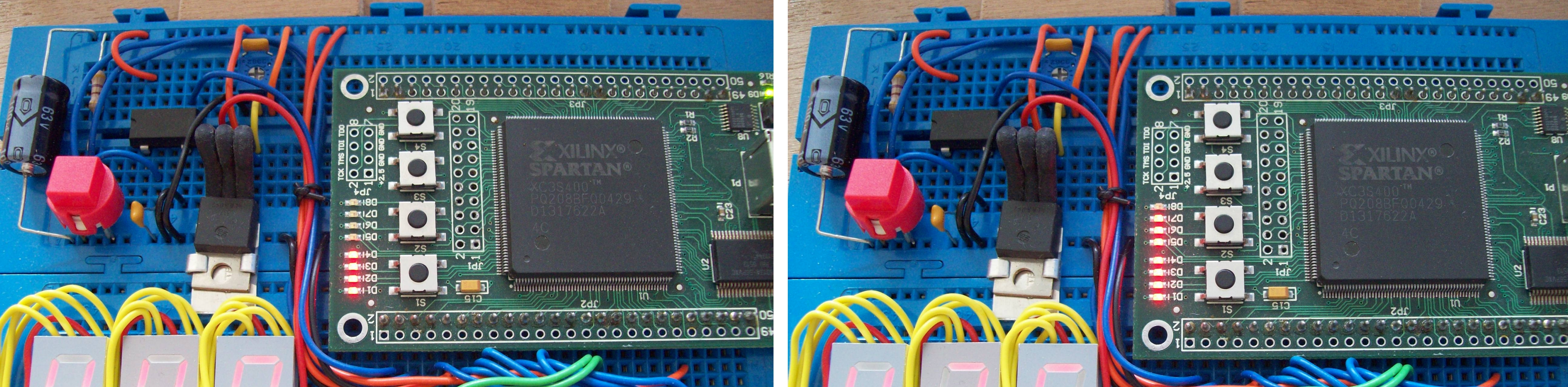
Figure 11 : LED bargrapgh
Port B is an 4bit input port connecting the PicoBlaze to the push buttons. The switch hardware is shown in figure 12. Port B has four push buttons, active low. The POLL switch is on PortB0, the INTERRUPT is on switch PortB3, connected to the interrupt line through an inverter. The RESET button has an additional debounce capacitor, again connected through an inverter to the processor's reset pin. To illustrate the steps involved in reading an input port consider the stripped down system shown in figure 13, i.e. only has input port B.
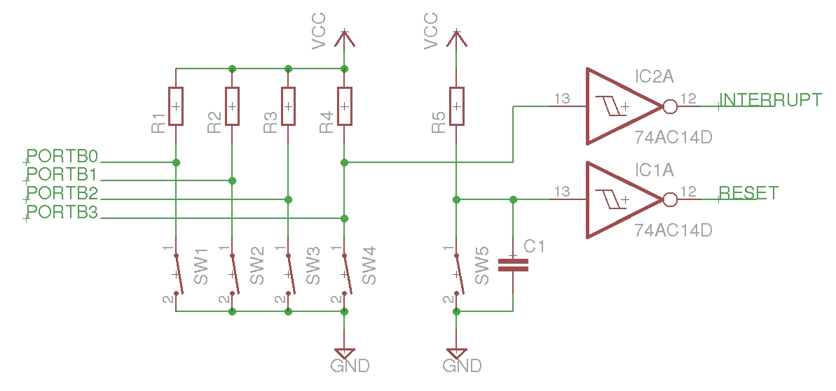
Figure 12 : Push buttons

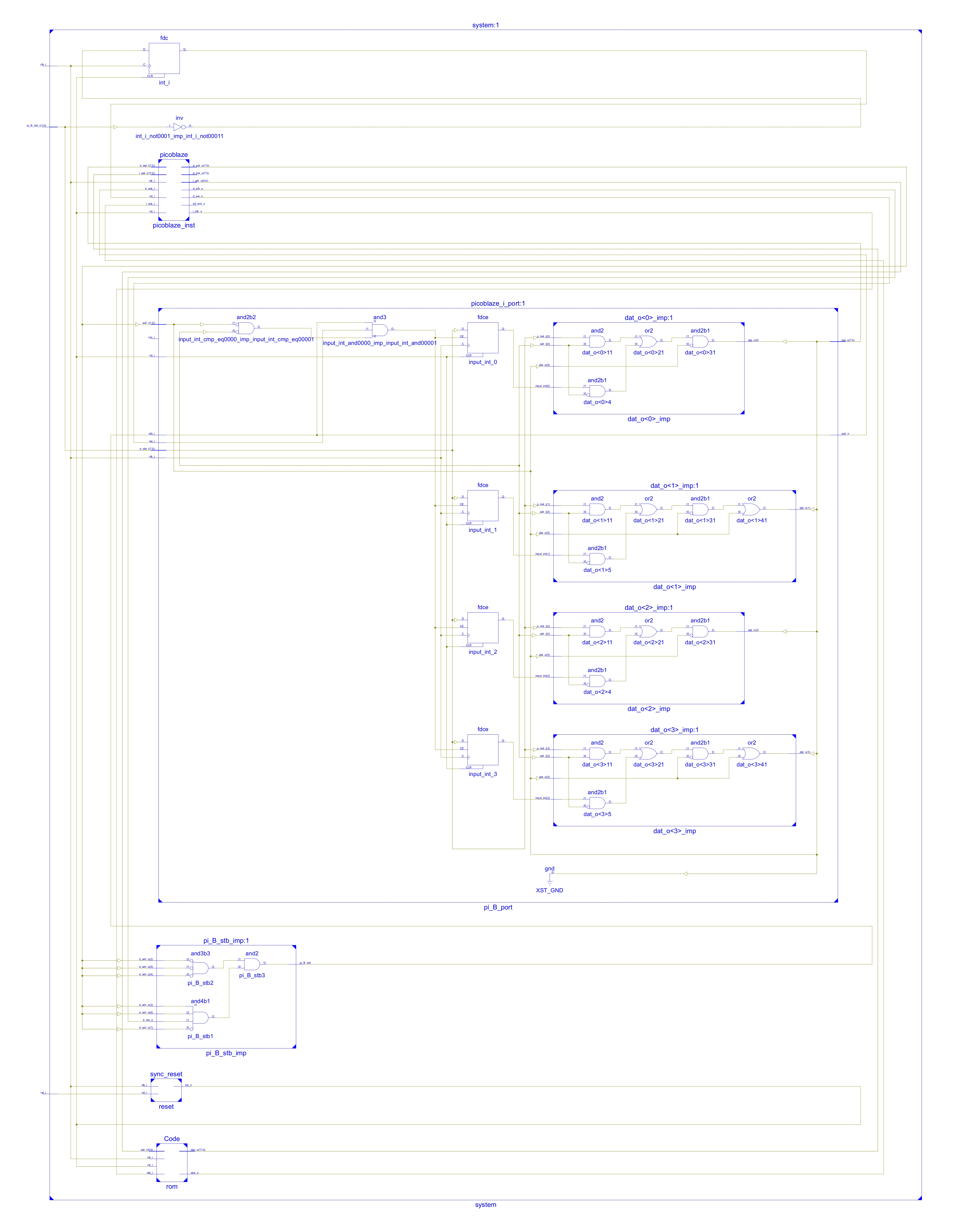
Figure 13 : Input port PicoBlaze system, block diagram (top), RTL schematic (bottom)
Port B is assigned the base memory address 72 decimal (0x48 hexidecimal, or 01001000b binary), using the address decoder shown in figure 14. The subroutine used to read this input port is shown below:
; *==========================================================
; * CONSTANT
; *==========================================================

	SW_PORT_REG  EQU 0x48;
	SW_PORT_BUF  EQU 0x49;

; *==========================================================
; * POLL INPUT PORT
; *==========================================================

poll:	IN SA, SW_PORT_BUF      ;read input port
	AND SA, 1		;mask switch bit
	RET NZ			;if zero not pressed
	LOAD SF, 0		;if pressed zero continue flag
	RET
When used in the stopwatch this subroutine reads the input port, storing the switch value in temporary register SA. Next, a bit mask (00000001b)is applied to select the desired bit i.e. PortB(0), performed using a bitwise AND. If the result is none zero the button has not been pressed and the subroutine returns. If it is zero, the global register SF is cleared, indicating that the stopwatch counter should be stopped. The input port shown in figure 15 is a little more complex than the output port, having four addressable locations i.e. the input port also decodes two address lines d_adr_o(1) and d_adr_o(0). The four active addresses are:
As the input port decodes the lower two address bits the address decoder for this peripheral (shown in figure 14) only decodes address lines d_adr_o(7) to d_adr_o(2), the bit pattern 010010XX, i.e. the data strobe line must be high for all active addresses (0x48 - 0x4B). Normally the raw input mode, address 0x48 is used to poll the push button status, however, if you need to capture the state of all the inputs the internal flip-flops can be used. These flip-flops are updated by writing to address 0x48. As this is an input port the data written by the processor is discarded, but the d_we_o control signal triggers the internal flip-flops to store the current value of port B. This data can then be accessed at any time by reading address 0x49. To aid in initial system debugging addresses 0x4A and 0x4B have been hard-wired to return the test pattern 0xAA, allowing the programmer to check the input port and its interconnecting buses. Note, the additional hardware connected to the flip-flop outputs show in figure 15 implements a multiplexer, allowing the processor to read either the raw, buffered (flip-flop), or hard-wired data (selected using address lines 0 and 1).
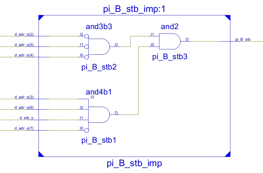
Figure 14 : Address decoder
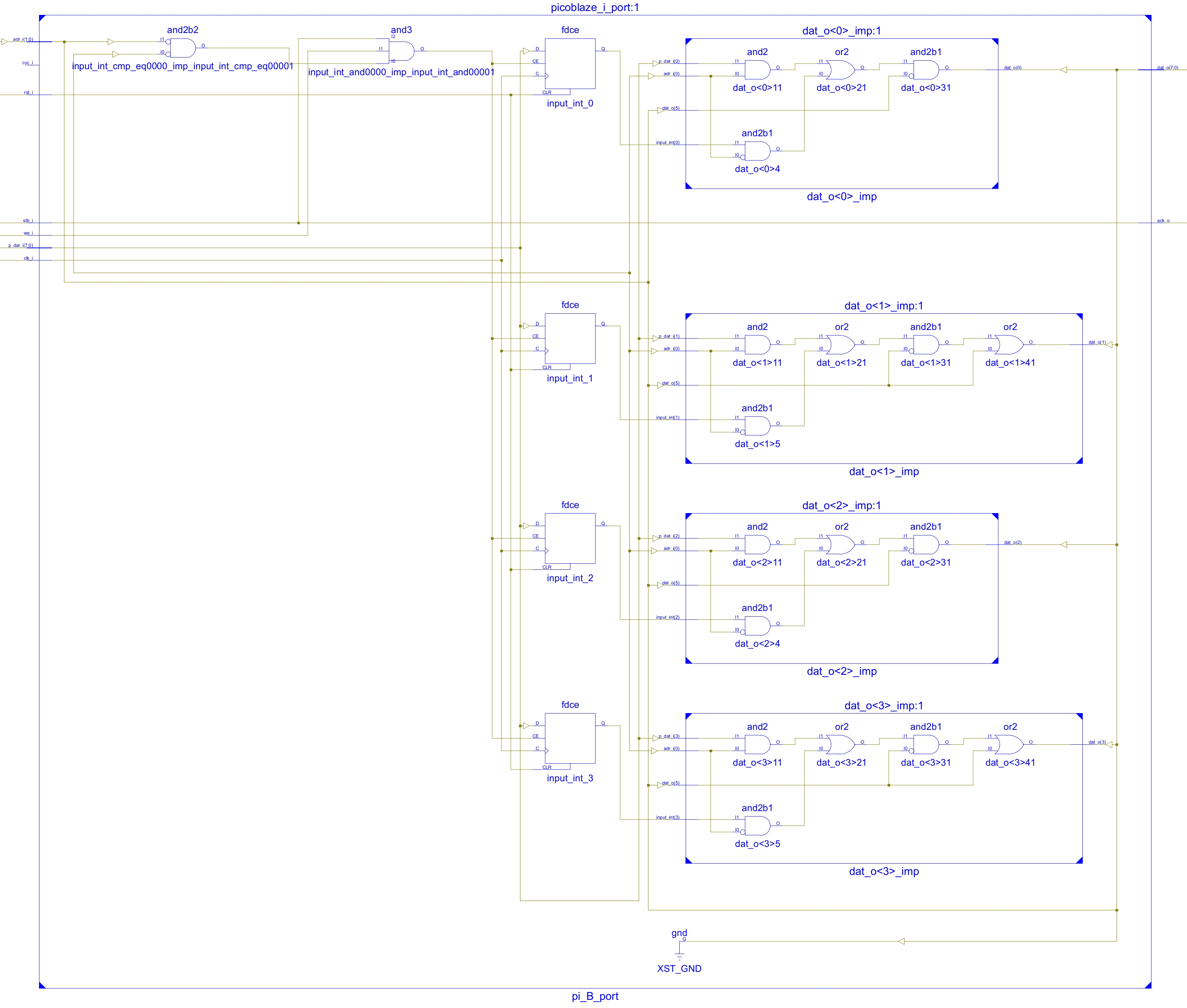
Figure 15 : Input port
As shown in figure 12 push button PortB3 is also used to drive the processor's interrupt line int_i. Note, the inverter is inside the CPLD, shown in the top left of the schematic in figure 12, this signal is also synchronised to the system's clock through a flip-flop. When the push button PortB3 is pressed a 0 -> 1 transition occurs on the interrupt line, causing the processor to jump to its interrupt vector i.e. address 0x3FF. More information on how the PicoBlaze responds to interrupt requests can be found here: (Link). The register SF is used as a global register, indicating if the stopwatch should keep counting i.e. 1=continue, 0=stop. Note SF is not used for any other purpose. When an interrupt occurs i.e. the stopwatch should stop, the interrupt service routine (ISR) simply has to clear this register.
; *==========================================================
; * INTERRUPT SERVICE ROUTINE
; *==========================================================

isr:	LOAD SF, 0		;zero continue flag
	RETI ENABLE		;return to main program

; *==========================================================
; * INTERRUPT VECTOR
; *==========================================================

ORG 0x3FF                       ;interrupt vector
	JUMP isr                ;jump to interrupt routine

; *==========================================================
; * END
; *==========================================================
The stopwatch program uses registers S0 and S1 to implement a 16bit counter i.e. to store the display value of 000 to 999 (a single 8bit register could only represent a value up to 255). However, this binary value needs to be converted into the decimal display digit format. Notes, perhaps a more efficient representation for the counter would be Binary Coded Decimal (BCD) i.e. does not need to be decoded. To convert this binary value into its decimal digits the code below repeatedly subtracts 1000 from the 16bit counter to determine the most significant digit i.e. it counts the number of 1000s that can be subtract from the counter before it goes negative. It then subtracts 100s and finally 10s from the 16bit counter (remainder will be units) to work out each digit's value. At the end of this subroutine the count value stored in register S0 and S1 is converted into binary values representing the decimal digits i.e. S6 stores the number of 1000s, S7 stores the number of 100s, S8 stores the number of 10s and S4 the units. Note, could remove the 1000s i.e. max value is 999.
; *==========================================================
; * UPDATE SEVEN SEGMENT DISPLAYS
; *==========================================================

; CONSTANTS
; ---------
; 1000 = 0x3E8
; 100  = 0x64
; 10   = 0x0A

update: LOAD S4, S0		;make copy of count
	LOAD S5, S1
	LOAD S6, 0		; zero 1000s count
	LOAD S7, 0		; zero 100s count
	LOAD S8, 0		; zero 10s count

loop1000:
	SUB S4, 0xE8		; subtract 1000
	SUBC S5, 0x03
	JUMP C, exit1000	; neg result?
	ADD S6, 01		; no inc count
	JUMP loop1000		; repeat

exit1000:
	ADD S4, 0xE8		; ADD 1000
	ADDC S5, 0x03

loop100:
	SUB S4, 0x64		; subtract 100
	SUBC S5, 0x00
	JUMP C, exit100		; neg result?
	ADD S7, 01		; no inc count
	JUMP loop100		; repeat

exit100:
	ADD S4, 0x64		; ADD 100
	ADDC S5, 0x00

loop10:
	SUB S4, 0x0A		; subtract 10
	SUBC S5, 0x00
	JUMP C, exit10		; neg result?
	ADD S8, 01		; no inc count
	JUMP loop10		; repeat

exit10:
	ADD S4, 0x0A		; ADD 10
	ADDC S5, 0x00
	CALL display		;update LED display

	RET
At the end of the update subroutine the display subroutine is called (shown below). This program translates the decimal digits into 7SEG values, writing these to Port A i.e. the 7SEG_PORT controller.
; *==========================================================
; * CONSTANT
; *==========================================================

	7SEG_PORT_0  EQU 0x40;
	7SEG_PORT_1  EQU 0x41;
	7SEG_PORT_2  EQU 0x42;
	7SEG_PORT_3  EQU 0x43;

; *==========================================================
; * CONVERT DIGIT TO SEVEN SEGMENT
; *==========================================================

display:
	LOAD S9, S4		; update 1s digit
	CALL conv
	OUT S9, 7SEG_PORT_0
	LOAD S9, S8		; update 10s digit
	CALL conv
	OUT S9, 7SEG_PORT_1
	LOAD S9, S7		; update 100s digit
	CALL conv
	OUT S9, 7SEG_PORT_2
	LOAD S9, S6		; update 1000s digit
	CALL conv
	OUT S9, 7SEG_PORT_3
	RET
The decimal digit to be displayed on a seven segment LED is transferred to register S9, the code below converts this value into the correct seven segment pattern i.e. each bit controls one of the LED segments: 0=OFF, 1=ON. The seven segments of each digit: A,B,C,D,E,F and G are controlled by a CPLD connected to Port A. Note, a more efficient method to implement this translation from decimal digit to 7SEG pattern would be a lookup table e.g. memory location 0=0xFE, 1=0x60, 2=0xDA etc, register R9 can then be used to index this table.
; *==========================================================
; * CONVERT DIGIT TO SEVEN SEGMENT
; *==========================================================

; SEVEN SEGMENT DISPLAY
;
;	   AAA
;	F	B
;	F	B
;	F	B
;	   GGG
;	E	C
;	E	C
;	E	C
;	   DDD
;
; DIGIT		    OUTPUTS	    HEX
;  		a b c d e f g dp
;   0           1 1 1 1 1 1 0 0	    0xFE
;   1           0 1 1 0 0 0 0 0     0x60
;   2           1 1 0 1 1 0 1 0	    0xDA
;   3           1 1 1 1 0 0 1 0     0xF2
;   4           0 1 1 0 0 1 1 0     0x66
;   5           1 0 1 1 0 1 1 0     0xB6
;   6           1 0 1 1 1 1 1 0     0xBE
;   7           1 1 1 0 0 0 0 0     0xE0
;   8           1 1 1 1 1 1 1 0     0xFE
;   9           1 1 1 1 0 1 1 0     0xF6
;   BLANK       0 0 0 0 0 0 0 0     0x00

conv:
	AND S9, 0xFF		;is count 0?
	JUMP NZ, conv1
	LOAD S9, 0xFC
	RET
conv1:	COMP S9, 1		;is count 1?
	JUMP NZ, conv2
	LOAD S9, 0x60
	RET
conv2:	COMP S9, 2		;is count 2?
	JUMP NZ, conv3
	LOAD S9, 0xDA
	RET
conv3:	COMP S9, 3		;is count 3?
	JUMP NZ, conv4
	LOAD S9, 0xF2
	RET
conv4:	COMP S9, 4		;is count 4?
	JUMP NZ, conv5
	LOAD S9, 0x66
	RET
conv5:	COMP S9, 5		;is count 5?
	JUMP NZ, conv6
	LOAD S9, 0xB6
	RET
conv6:	COMP S9, 6		;is count 6?
	JUMP NZ, conv7
	LOAD S9, 0xBE
	RET
conv7:	COMP S9, 7		;is count 7?
	JUMP NZ, conv8
	LOAD S9, 0xE0
	RET
conv8:	COMP S9, 8		;is count 8?
	JUMP NZ, conv9
	LOAD S9, 0xFE
	RET
conv9:	COMP S9, 9		;is count 9?
	JUMP NZ, conv10
	LOAD S9, 0xF6
	RET
conv10:	LOAD S9, 0x00		; error blank display
	RET
Port A is a complex output port, assigned the base address 64 decimal (0x40 hexadecimal, or 01000000b binary). When an 8bit value is written to this address it is passed to the CPLD over an external bus. To illustrate the steps involved in writing data to the LEDS consider the stripped down system shown in figure 16, i.e. only has output port A.
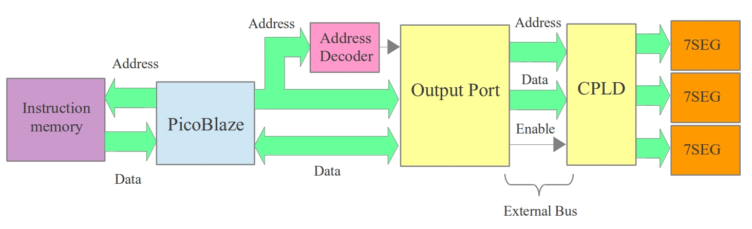
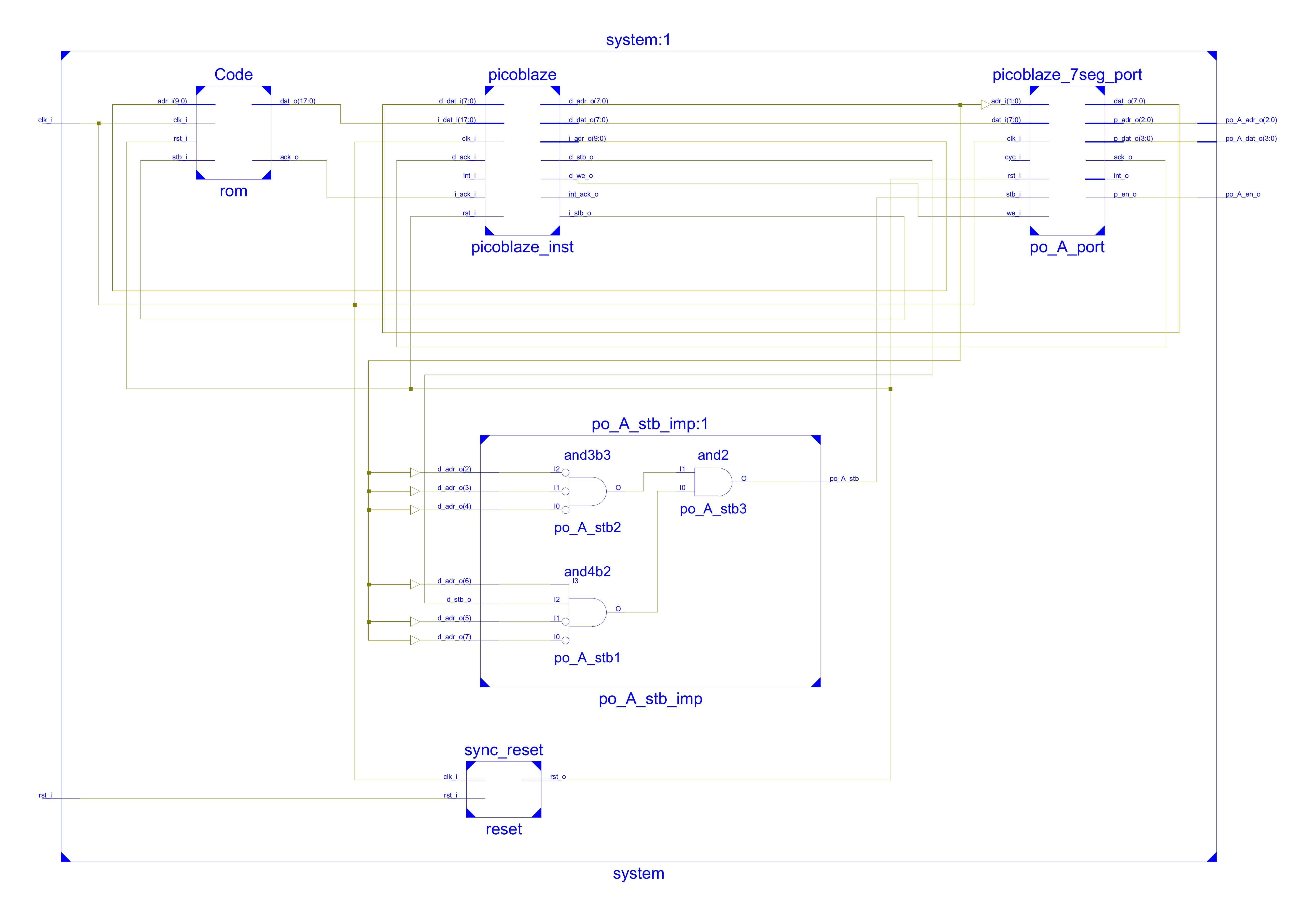
Figure 16 : Port A architecture, block diagram (top), RTL schematic (bottom)
Port A contains a simple state machine that takes the 8bit value written to it, partitions this into two 4bit nibbles, then using the lower 2bits of the base address as the external address (0x40=0, 0x41=1, 0x42=2 and 0x43=3), sequentially writes the two 4bit nibbles to the CPLD flip-flops. The CPLD hardware contains 12 flip-flop, controlling the three seven segment displays. The first four CPLD flip-flops and their decoding hardware are shown in figure 17, the full circuit diagram can be viewed here: (Link).
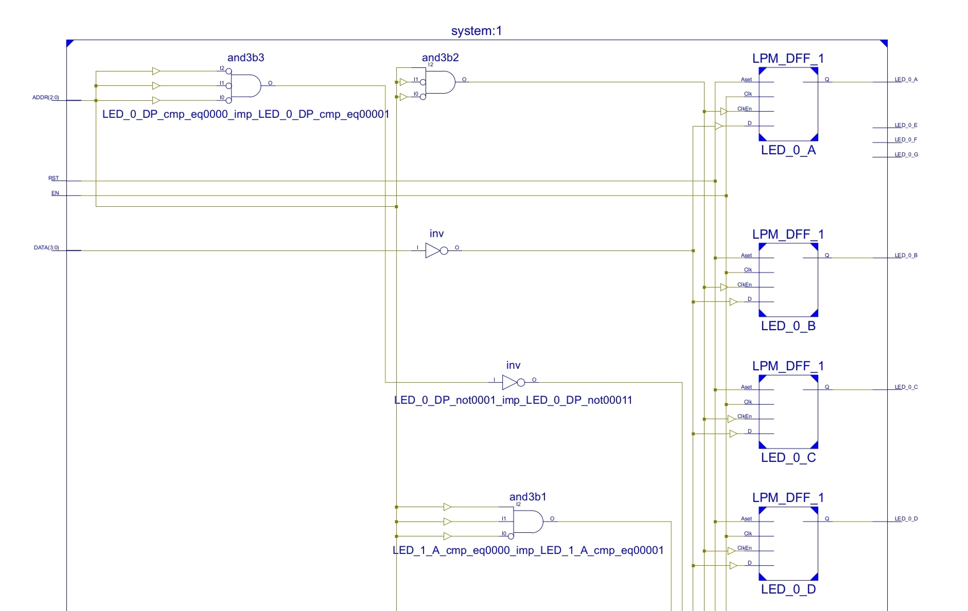
Figure 17 : CPLD hardware (first four bits)
The state machine behaviour is defined by the state diagram shown in figure 18. Simulations of the external data bus transfers are shown in figures 19 and 20. Note, the address bus (po_A_adr_o) selects the flip-flop bank (4 bits) to be updated, the enable signal (po_A_en) then clocks the data on the data bus (po_dat_o) into these flip-flops. To ensure that the correct bank is updated and that the correct data is stored, the address and data buses are not changed until the enable signal has be returned back to a logic 0. The sequence of events involved in this transfer as described below:
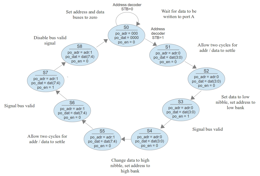
Figure 18 : State diagram
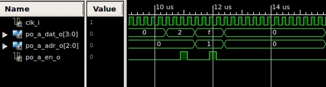
Figure 19 : External bus transferring '3' to the units LED
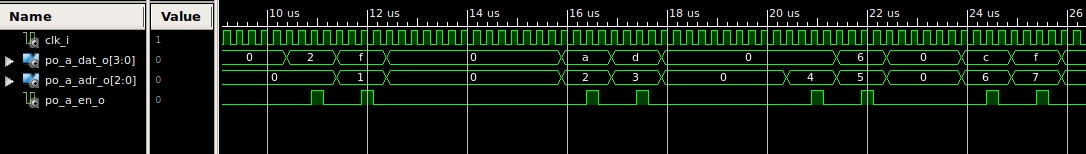
Figure 20 : External bus transferring LED value 0123
The final segment of code needed to implement the stopwatch is shown below. The stopwatch count is stored in registers S0 and S1. The constant 0x0001 is stored in registers S2 and S3. The register SF is used as a global register, indicating if the stopwatch should keep counting i.e. 1=continue, 0=stop. Note SF is not used for any other purpose. The program next enables interrupts and enters the main loop. The value 0x0001 is added to the counter using the 16bit add subroutine add16. The program then calls the previously described subroutines, updating the display and testing the STOP push buttons. The full program is available here: (Link).
; *==========================================================
; * MAIN
; *==========================================================

start:	LOAD S0, 0		; 16bit number A LSB
	LOAD S1, 0		; 16bit number A MSB
	LOAD S2, 1		; 16bit number B LSB
	LOAD S3, 0		; 16bit number B MSB

	LOAD SF, 1		; set repeat flag to TRUE
	EINT                    ; enable interrupts

loop:
	CALL add16		; increment count
	CALL update 		; update seven segment display
	CALL delay		; wait 1 second
	CALL poll		; test STOP button

	AND SF, 1		; continue?
	JUMP NZ, loop

trap:	JUMP trap		; halt

; *==========================================================
; * ADD 16
; *==========================================================
add16:	ADD S0, S2		; perform 16bit addition
	ADDC S1, S3
	RET                     ; return back to main program
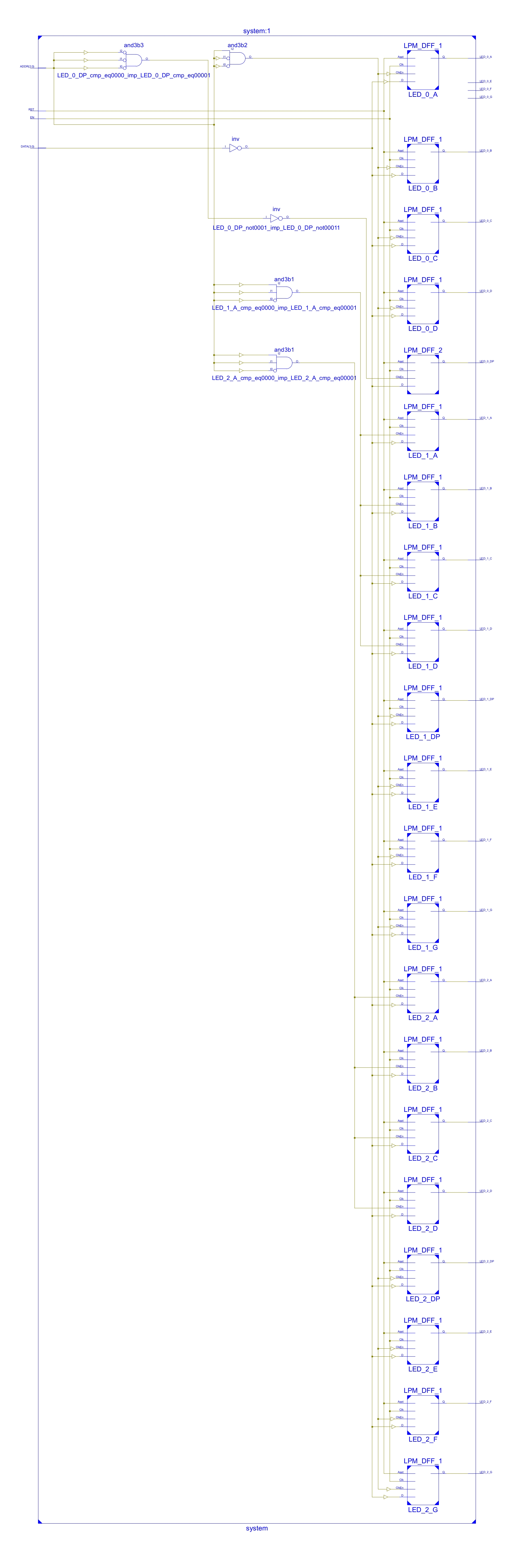
The complete system schematic is shown in figure 21. Address decoders have been moved into a new component: address_decoder16, same hardware as previous described, just tidied up. The only new component is system_bus_mux16. In all the previous example systems there is only one component writing information back to the processor i.e. driving data onto d_dat_i bus. However, in the final system all three ports need to access this bus. If these peripherals were simply all connected to this shared bus data collisions would occur i.e. you can not write a logic 1 and logic 0 to the same wire at the same time, VERY BAD THINGS WILL HAPPEN. Therefore, an 8bit multiplexer is used. The output from the address decoder drives this hardware component, connecting the active (selected) port to the processor's data input bus i.e. each port has a different address, therefore, only one address decoder will be active, therefore, only one port will be connected to this bus at a time. Note, in the old days we used bi-directional buses with tri-state buffers (Link), in these cases you switched each peripheral device on-and-off the shared bus (wires). Implementing a multiplexer using tri-state buffers slows down bus transactions as you need a turn-around period where no device is driving the bus. Modern FPGA design tend to use logic based multiplexer as it simplifies designs, minimises bus length (routing) and therefore increases speed.
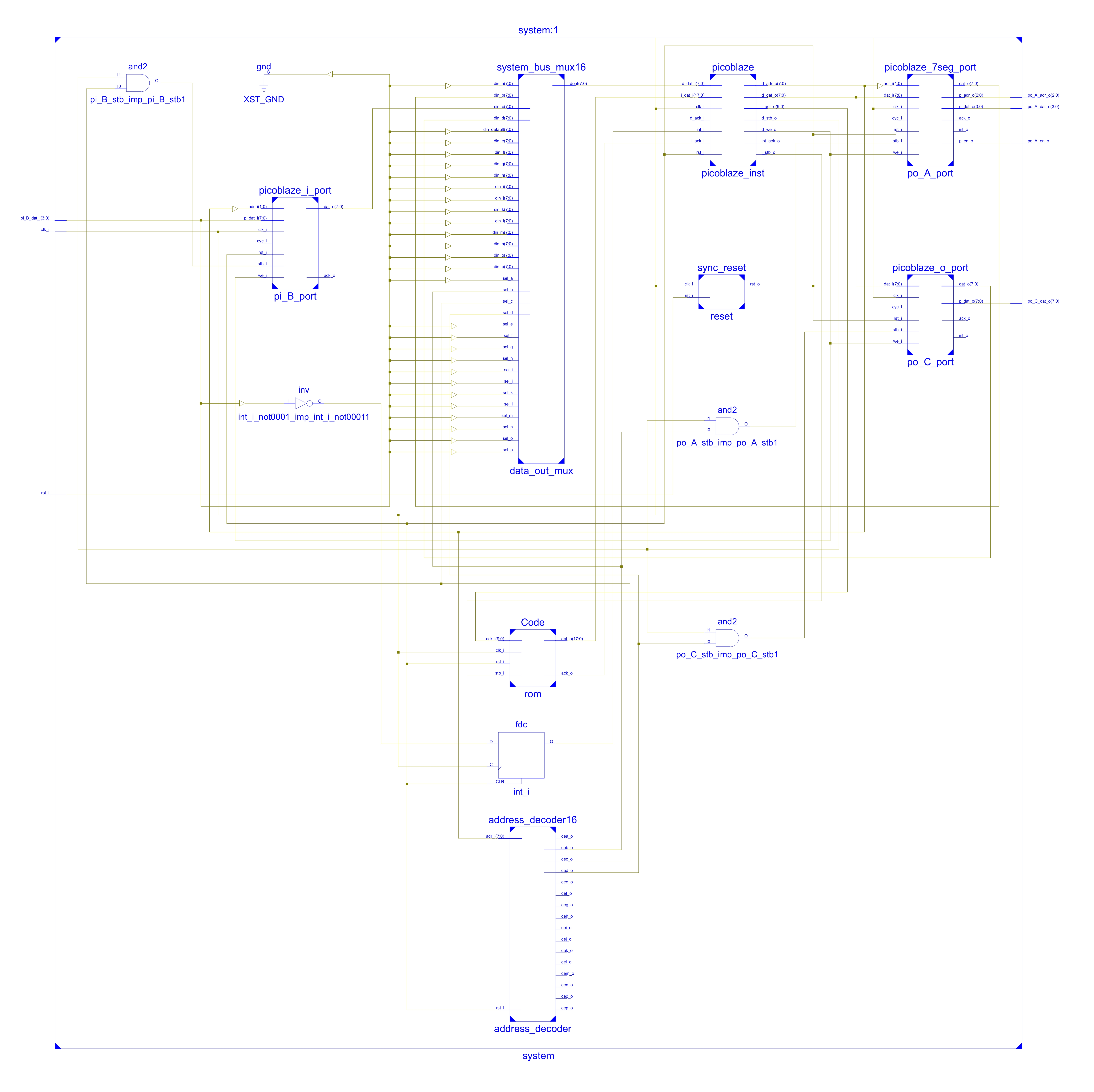
Figure 21 : Final system
The aim of this demo is to show the differences between interrupts and polling. When in operation if you press the polled stop button whilst the program is in the software delay routine, this request will be missed as the switch is not polled during this routine e.g. if you were tp press and release the push button whilst the thermometer scale LED bar-graph is in the middle. If you press the interrupt stop button the count will stop straight away as the system will always respond to the interrupt request. However, if you were to press and hold the interrupt stop button the system would never leave the software delay loop i.e. the bar-graph would not reach the top until this button is released. This illustrates one of the disadvantages of an interrupt based system i.e. constant or high frequency interrupts prevent the main program from running i.e. you will always be 'stuck' in the interrupt service routine. This is not a significant problem for this example, but consider what would happen if a lap timer mode was added. In this example you want the timer to continue, each time the button is pressed the system would display the time of the previous lap or the total accumulated time. If an interrupt based system was used, holding down the interrupt button would lock the system, the program will repeatedly call the interrupt service routine and never return to the main program i.e. the count would stop. Using a polling based system would allow the count to continue i.e. the system explicitly tests the switch state, it is not forced to test the switch as in the case of an interrupt. Note, a simple solution to this problem would be to add addition hardware to change the current level sensitive interrupt line to a edge sensitive interrupt i.e. the transition from a 0 -> 1 generates an interrupt, not the logical state of the signal.

This work is licensed under a Creative Commons Attribution-NonCommercial-NoDerivatives 4.0 International License.
Contact details: email - mike.freeman@york.ac.uk, telephone - 01904 32(5473)
Back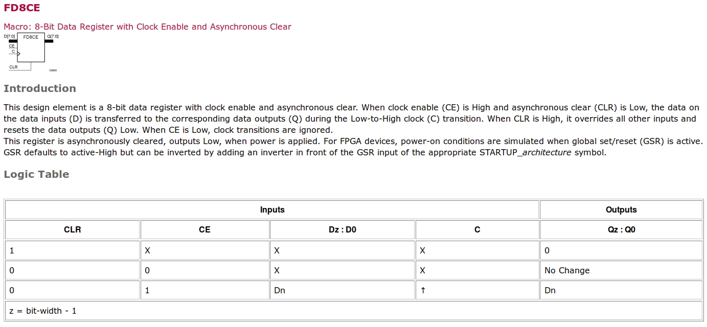